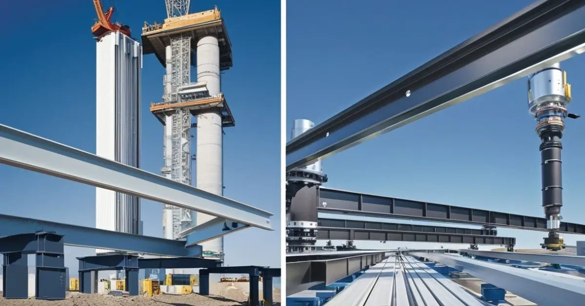
Beam inspection plays a vital role across industries, ensuring the safety, reliability, and efficiency of materials and structures. From towering constructions to microscopic semiconductor components, inspecting beams for defects, alignment, and structural integrity is a critical process that supports modern advancements.
This article delves into the meaning, applications, and techniques of beam inspections, highlighting how they contribute to safety and precision in construction and manufacturing.
Understanding Beam Inspection
Beam inspection refers to the evaluation and analysis of beams to identify flaws, measure dimensions, or verify compliance with design specifications. This inspection can occur on a macro scale, such as in buildings and bridges, or a micro scale, such as in semiconductor wafers. It is carried out using advanced techniques to ensure optimal performance and safety.
Key Areas of Beam Inspection:
- Structural Beams: Common in construction, these beams include steel, concrete, and composites that need regular inspection to maintain structural integrity.
- Electron Beam (E-Beam) Technology: Used in electronics and semiconductor manufacturing, e-beam inspections help detect microscopic defects in highly complex devices.
Applications of Beam Inspection
1. Structural Beam Inspection in Construction
Structural beams form the backbone of any building, bridge, or industrial facility. Inspections focus on ensuring the material strength and alignment to handle loads effectively.
Common Methods:
- Visual Inspection: Observing surface-level defects like cracks, corrosion, or deformation.
- Ultrasonic Testing (UT): Utilizing sound waves to locate internal defects.
- Magnetic Particle Testing (MPT): Effective for detecting flaws in ferromagnetic materials.
- Radiographic Testing (RT): X-rays reveal deeper, hidden issues.
Key Benefits:
- Safety Assurance: Prevents potential disasters caused by structural failure.
- Compliance: Meets building codes and industry standards.
- Longevity: Identifies early-stage deterioration to extend the life of structures.
2. Electron Beam Inspection in Semiconductors
As industries push for smaller and more powerful electronic devices, the manufacturing of semiconductors demands exceptional precision. E-beam inspections allow manufacturers to analyze wafers at the nanometer level, detecting defects that could impact device performance.
Applications in Electronics:
- Defect Detection: Identifies flaws in microscopic patterns, such as missing or misaligned features.
- Critical Dimension (CD) Metrology: Ensures that dimensions match design tolerances.
- Overlay Inspection: Verifies the alignment of layers in multilayer semiconductor devices.
Advantages:
- High Sensitivity: Detects defects as small as 1 nanometer.
- Speed: Advanced systems enable high-throughput analysis.
- Adaptability: Suitable for emerging technologies like 3D NAND and FinFET devices.
Techniques in Beam Inspection
Beam inspections rely on a mix of traditional and cutting-edge techniques tailored to specific applications. These methods ensure comprehensive coverage and reliability in identifying defects.
Techniques for Structural Beam Inspection:
- Non-Destructive Testing (NDT): Techniques such as UT and RT allow inspectors to evaluate beams without causing damage.
- Load Testing: Simulates the stresses that beams would encounter in real-world conditions.
- Digital Twin Analysis: Combines real-time data with digital simulations to predict potential issues.
Techniques for E-Beam Inspection:
- Secondary Electron Imaging: Uses low-energy electrons to capture high-resolution images of surfaces.
- Backscattered Electron Detection: Identifies deeper structural flaws by analyzing reflected electrons.
- AI Integration: Speeds up defect categorization through automated image analysis.
Innovations Driving Beam Inspection
Advances in Structural Beam Inspection:
- Portable NDT Devices: Compact tools that allow for on-site, rapid inspections.
- AI and Machine Learning: Enhance the detection of anomalies in visual inspections.
- Automated Robotics: Perform inspections in hard-to-reach areas, reducing human risk.
Evolving E-Beam Technology:
- Multi-Beam Systems: Combine multiple beams to increase throughput without compromising resolution.
- AI-Powered Analysis: Reduces inspection time by automating defect detection and classification.
- Edge Placement Error (EPE) Metrics: Help identify and correct alignment issues in advanced semiconductors.
Challenges in Beam Inspections
While beam inspections are indispensable, they come with challenges:
- High Costs: Advanced techniques like e-beam inspections demand significant investment in equipment and training.
- Throughput Limitations: Balancing speed with precision remains a challenge, particularly for large-scale applications.
- Technical Expertise: Both structural and e-beam inspections require specialized knowledge for accurate results.
Comparison of Structural and E-Beam Inspections
| Feature | Structural Beam Inspection | E-Beam Inspection |
|---|---|---|
| Primary Application | Ensures structural safety and durability | Ensures defect-free semiconductor devices |
| Techniques | Visual, UT, RT, MPT | Secondary electron imaging, AI |
| Resolution | Millimeter-scale | Nanometer-scale |
| Inspection Area | Buildings, bridges | Semiconductor wafers |
| Advantages | Prevents accidents, complies with codes | High yield, unmatched precision |
The Role of Beam Inspection in Safety and Quality
Structural Safety
In construction, beam inspections are integral to maintaining the structural integrity of buildings and infrastructure. By detecting and addressing issues early, inspections prevent catastrophic failures.
Manufacturing Precision
In semiconductor manufacturing, the margin for error is minuscule. Beam inspections ensure that every chip meets stringent quality standards, enhancing the performance and reliability of electronic devices.
Conclusion
Beam inspections are foundational to modern engineering and technology, safeguarding structures and ensuring the flawless operation of advanced electronics. Whether for towering bridges or microscopic semiconductors, inspections combine precision, innovation, and reliability to support progress.
These processes continue to evolve, driven by advancements in AI, robotics, and high-resolution imaging, promising a future where inspections are faster, more efficient, and even more reliable.


